Article Sections
Graphene micromesh for transparent conductive films application
Loading author information...
Graphical Abstract & Abstract
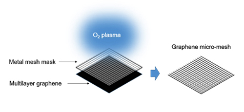
In order to improve the properties of the graphene transparent conductive film, we developed a process of O2 plasma patterning graphene using a metal mesh as an etching mask. The CVD growth conditions of high-quality multilayer graphene samples consisting of 400 layers or more were found using Ni foil, and the R sheet = 3.4 ± 0.6 Ω/sq. was achieved. The best performance of graphene micromesh based transparent conductive films so far was R sheet = 22.2 Ω/sq. at T = 47.1 ± 1.9 %. According to theoretical calculations based on the combined resistance of the two-dimensional resistance lattice circuit, a combined resistance of 46.8 Ω can be realized at T = 90%.
How to Cite
(2019). Graphene micromesh for transparent conductive films application. Advanced Materials Letters, 10(6), 417-420. https://doi.org/10.5185/amlett.2019.2238