
Article Sections
Effect of Incident Light on Transport Properties of Pulsed Laser Deposited Manganite Thin Films
Loading author information...
Graphical Abstract & Abstract
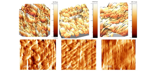
In this communication, we report the results of different light illumination on electrical transport properties of La0.67Ca0.33Mn0.9Ga0.1O3 (LCMGO) thin films grown on Si (100) ( n-type phosphorus-doped) wafer using Pulsed Laser Deposition (PLD) System. The variation in deposition time changes the thickness of the films. X-ray Diffraction (XRD) reveals the polycrystalline structure of LCMGO thin films. The cross-sectional SEM were taken to determine the thickness of the films with changing deposition time. Atomic Forced Micrographs (AFM) show that island type grains diffuse into one another to form a more uniform distribution of grains as the thickness of the film increases. The charge transport properties have been studied using the I-V measurement at LCMGO/Si interfaces. I-V measurement shows the backwards-diode like the behaviour of the LCMGO/Si p-n junction. The reverse bias current changes under the influence of different incident light illumination. The built-in electric field is
How to Cite
(2020). Effect of Incident Light on Transport Properties of Pulsed Laser Deposited Manganite Thin Films. Advanced Materials Letters, 11(4), 1-5. https://doi.org/10.5185/amlett.2020.041502