
Article Sections
Narrow bandgap quantum dot diode structures and photoresistors for thermo-photovoltaic and infrared applications
Loading author information...
Graphical Abstract & Abstract
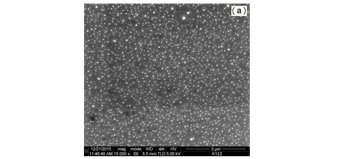
For the thermophotovoltaic (TPV) and other mid-infrared applications, the narrow bandgap quantum dot (QD) diode structures and photoresistors (PR) based on InAsSbP alloys and InAs industrial substrates are fabricated and investigated. For the nucleation of InAsSbP composition strain-induced QDs in Stranski–Krastanow growth mode, as well as at the growth of emitter epilayer lattice-matched with the InAs(100) substrate, the modified liquid phase epitaxy (MLPE) technique is employed. The HR-SEM and AFM microscopes are used for characterization. The grown QDs surface density equals to (3-8)×109 cm -2 , with height and width dimensions ranges from 4 nm to 15 nm and 10 nm to 35 nm, respectively. The current-voltage characteristics and photoresponse spectra of QD TPV and PR structures are also explored. The redshift of the absorption edge, as well as enlargement toward the short wavelength region is revealed for both QD-based devices. The quantitative calculations show increasing of QD-based
How to Cite
(2018). Narrow bandgap quantum dot diode structures and photoresistors for thermo-photovoltaic and infrared applications. Advanced Materials Letters, 9(2), 112-115. https://doi.org/10.5185/amlett.2018.1804