
Article Sections
Waveguide-detector system on silicon for sensor application
Loading author information...
Graphical Abstract & Abstract
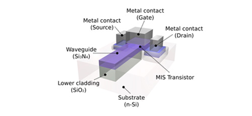
A whole silicon monolithic waveguide-detector system is studied. Four different coupling electrophotonic devices are presented. One of them is analyzed in detail. The studied system consists of a planar p-n junction with a waveguide built in a cavity in front of it. The output port of the waveguide faces directly to the depleted layer maximizing absorbance of all photons. The waveguide is experimentally fabricated and characterized, and light on the visible range is transmitted in multimode. The simulation of the fabrication process considers an N-type silicon substrate, whose resistivity is varied from 10Ω×cm to 1000Ω×cm. The diode sensor is characterized by computational simulation, and the model is validated using characteristics of diodes previously fabricated. The dark current, the electric field and the characteristics of the depleted zone are obtained to optimize the design of the system. Electrical stimulations are performed for bias voltages of 0 V, -5 V, -10 V, -20 V and -30
How to Cite
(2018). Waveguide-detector system on silicon for sensor application. Advanced Materials Letters, 9(2), 116-122. https://doi.org/10.5185/amlett.2018.1552