
Article Sections
Work function and induced band bending characterization for engineering of selective contact for solar cells
Loading author information...
Graphical Abstract & Abstract
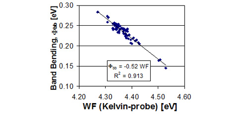
This work demonstrates the effectiveness of non-contact Kelvin-probe and surface photovoltage characterization of the work function (WF) induced barriers formed in silicon (Si) by thin 5nm carrier selective contact films of MoOx, TiO2 and MgF2. The calibrated Kelvin probe in the dark and under strong illumination where used to determine the dark WF of the deposited films and the band bending in the Si, FBB = WFDark – WFLight. The ac-surface photo voltage provided an independent measurement of the Si depletion layer width. Whole wafer mapping of all parameters can be performed. For n-type Si the high work function oxides MoOx (WF~5.7eV) and TiO2 (WF~5.0eV) are found to induce a depletion barrier with the height increasing with WF as FBB[eV] = 0.23WF – 0.77, i.e. quite similar to the well-known relationship for metal-silicon contacts. For the low work function MgF2 film, a depletion barrier was induced only in p-type Si. For this case, full wafer mapping revealed a lower WF pattern
How to Cite
(2018). Work function and induced band bending characterization for engineering of selective contact for solar cells. Advanced Materials Letters, 9(9), 629-631. https://doi.org/10.5185/amlett.2018.2084